
Mitsui Mining & Smelting has announced the opening of a new facility to manufacture its High Resolution Debondable Panel (HRDP), a speciality carrier for semiconductor packaging.
This expansion effort is being carried out by Mitsui Mining & Smelting, AKA Mitsui Kinzoku, in collaboration with GEOMATEC, a thin-film technology manufacturer.
Go deeper with GlobalData

Discover B2B Marketing That Performs
Combine business intelligence and editorial excellence to reach engaged professionals across 36 leading media platforms.
Both companies have been working in close coordination to establish and open a mass production system to support HRDP’s commercialisation.
This will be the second production line at GEOMATEC’s Ako plant in Japan. It is expected to become operational in 2025.
Simultaneously, GEOMATEC is also planning to make an investment in the thin-film process that will be used on this second line.
The entire capital investment strategy is scheduled to be executed gradually in steps between 2023 and 2025.
Furthermore, the facility expansion will boost the overall production capacity of Mitsui Kinzoku’s speciality carrier for next-generation semiconductor packaging, as well as enhance the operations of the Design of Experiments facility.
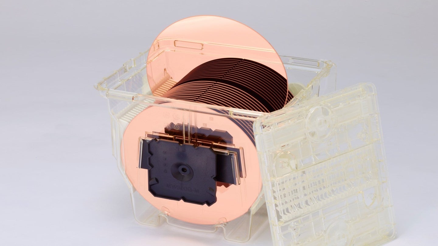
HRDP is a speciality carrier developed by Mitsui Kinzoku to meet the requirements of ultra-high-density design, having an L/S of 2/2μm or less, which is crucial for next-generation semiconductor packaging.
The latest expansion effort has been announced by Mitsui Kinzoku in response to the recent rise in full-scale developments of next-generation semiconductor packages by several semiconductor companies which are now leveraging HRDP technology.
According to Mitsui Kinzoku, the second production line will enhance and increase their production quality and capacity whilst ensuring that the companies can expedite joint development with other semiconductor organisations using HRDP.
This will also help in reducing the overall cycle times, a combination of processes and time required to develop a semiconductor package.
Once this cycle is minimised, the companies can achieve higher semiconductor device manufacturing efficiency.
The two companies will also be able to address the increasing demand for the development and adoption of HRDP while expanding its use in the mass production of next-generation semiconductors in the future.
